NVLink 1st-generation
NVIDIA NVLINK was unveiled by in March 2014 at the GPU Technology Conference (GTC) and released in 2016 with Pascal P100 that overcame throughput of PCI express 3.0
AIHARDWARE COMPUTERSTECHNOLOGY
Eduardo Domínguez Menéndez
8/7/20243 min read


This is the second article of the serie "The path to H100". This article will deep in one of the "miracles", like Jensen Huang referred to this technology, that enabled the P100.
Unveiled by NVIDIA in March 2014 at the GPU Technology Conference (GTC), NVLink represented a paradigm shift in chip-to-chip communications. NVLink was designed as an alternative solution to PCI Express with higher bandwidth and additional features.
Prior to the introduction of NVLink with Pascal (e.g., Kepler), multiple Nvidia GPUs would sit on a shared PCIe bus. Although direct GPU-GPU transfers and accesses were already possible using Nvidia's Unified Virtual Addressing over the PCIe bus, as the size of data sets continued to grow, the bus became a growing system bottleneck.
NVLink was designed to replace the inter-GPU communication from going over the PCIe lanes. It's worth noting that NVLink was also designed for CPU-GPU communication with higher bandwidth than PCIe. However, it's unlikely that NVLink can be implemented on an x86 system by either AMD or Intel.
In fact, prior to its integration into NVIDIA's Pascal architecture and other AI and HPC systems, NVLink was employed in IBM's Power8. This showcases how NVLink enables the integration of GPU-accelerated computing into server systems.
NVLink uses its proprietary High-Speed Signaling interconnect (NVHS). NVHS transmits data over a differential pair. This pair forms the atomic structure to transmit data inside an NVLink. Let's break down the composition from a GPU P100 until we reach the differential pair.
A P100 has 4 NVLinks. Each NVLink is bidirectional.
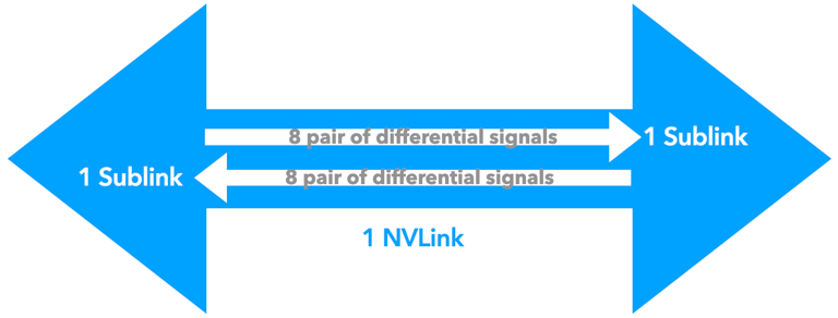
Now let's dissect a link: it is formed by two sublinks, each sublink is unidirectional.
The last step is a sublink: each one is comprised of eight differential signaling pairs. They operate in one direction.
We could think of a NVLink as a highway, a sublink as a one-way road of the highway, and each differential signaling pair as the lanes within the one-way road.
Let's see the throughputs of NVLink 1.0:
P100: 160 GB/s bidirectional and 80 GB/s unidirectional
Link: 40 GB/s bidirectional and 20 GB/s unidirectional
Sublink: 20 GB/s unidirectional (bidirectional not possible)
Differential signaling pair: 2.5 GB/s unidirectional (bidirectional not possible)

To provide context, at the beginning of the article, NVLink came to overcome PCIe limitations. Look at the figures by 2014: PCI Express 3.0 could achieve 15.7 GB/s across 16 lanes. Even with the advent of PCI Express 4.0 in 2017 and 5.0 in 2019, which reached 32 GB/s and 63 GB/s respectively, they fell short of what NVLink offered. This highlights the transformative potential of NVLink in overcoming the bandwidth and throughput limitations that have historically constrained system performance.
In conclusion, NVLink was not just a technological innovation; it was a strategic enabler for the next generations of computing architectures. It stands as a testament to NVIDIA's commitment to pushing the boundaries of what's possible, paving the way for advancements in artificial intelligence, deep learning, and high-performance computing that were once considered beyond reach.
You can watch the video version of this article here.